

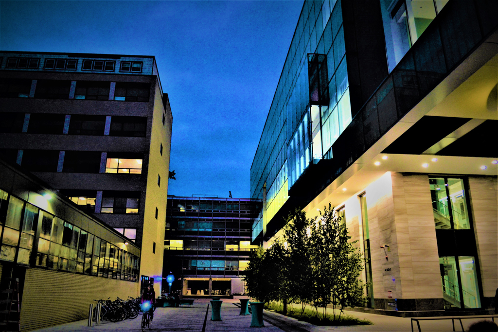
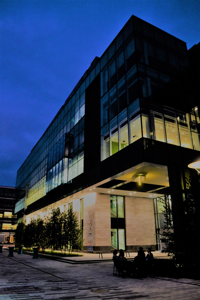
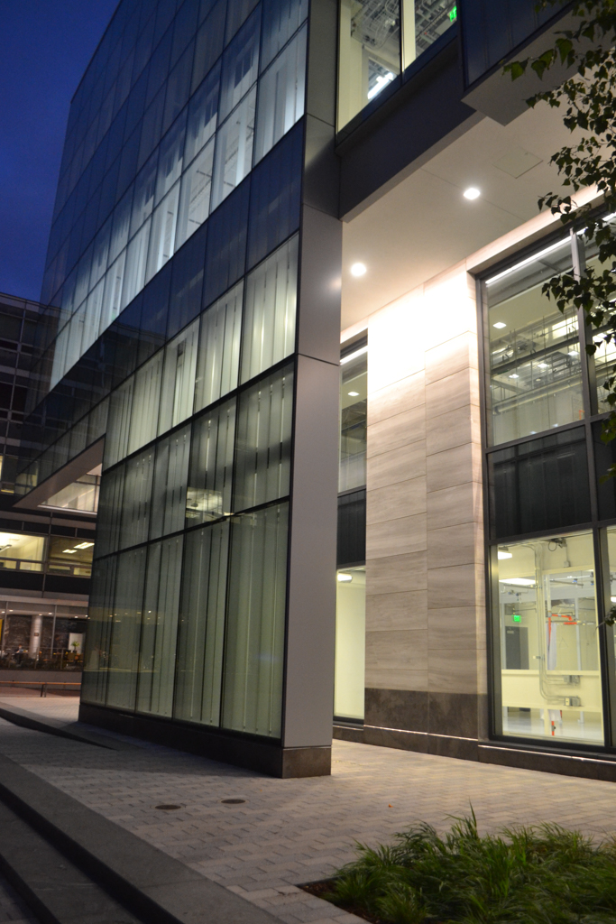
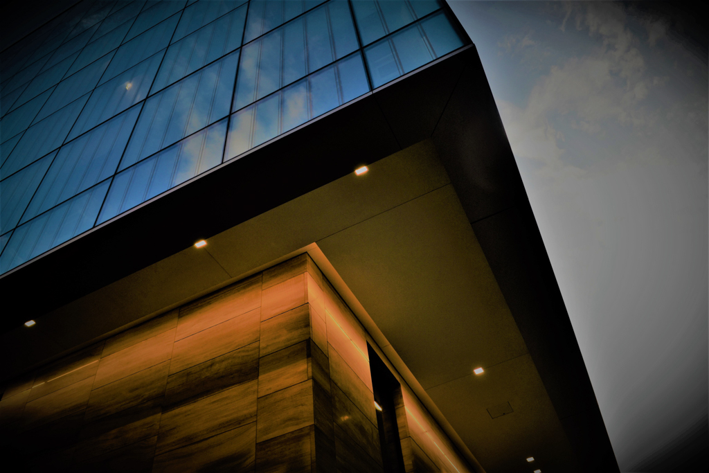
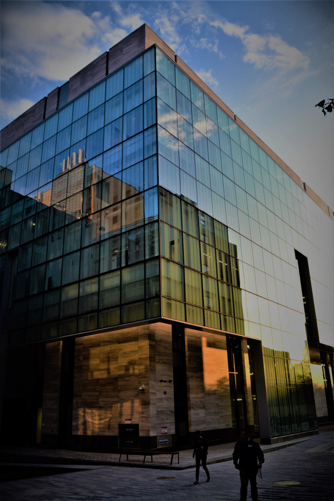
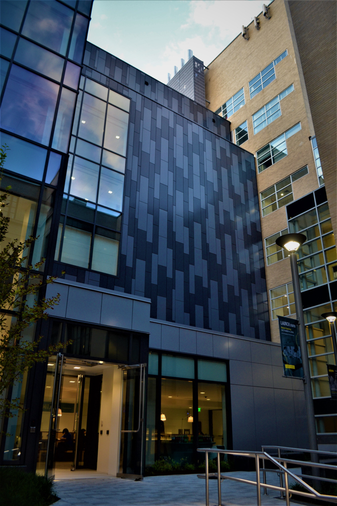
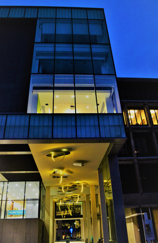
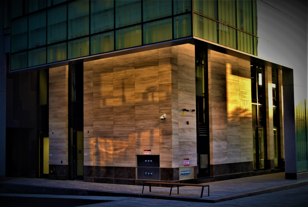
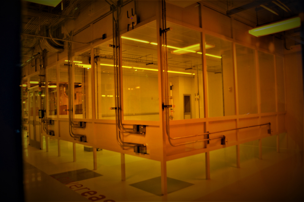
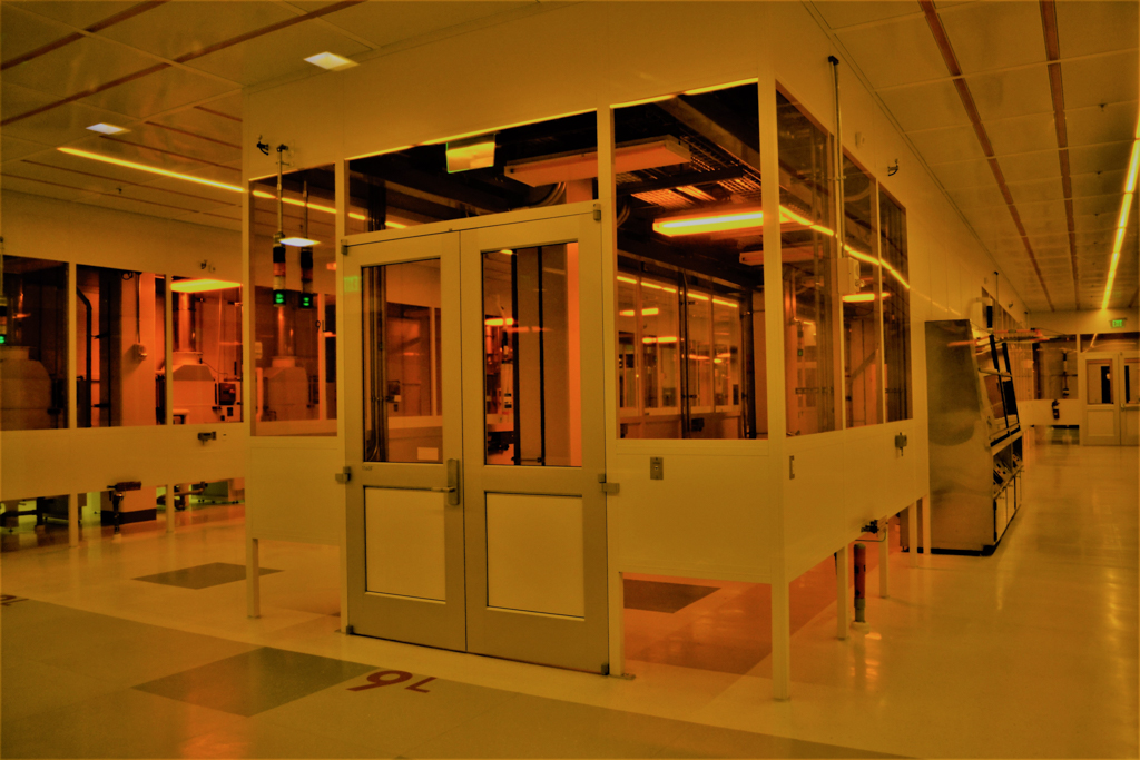
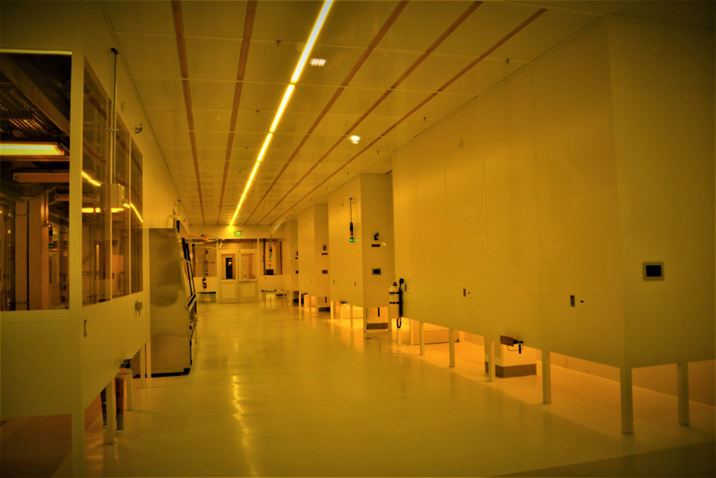
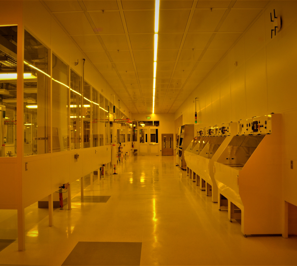
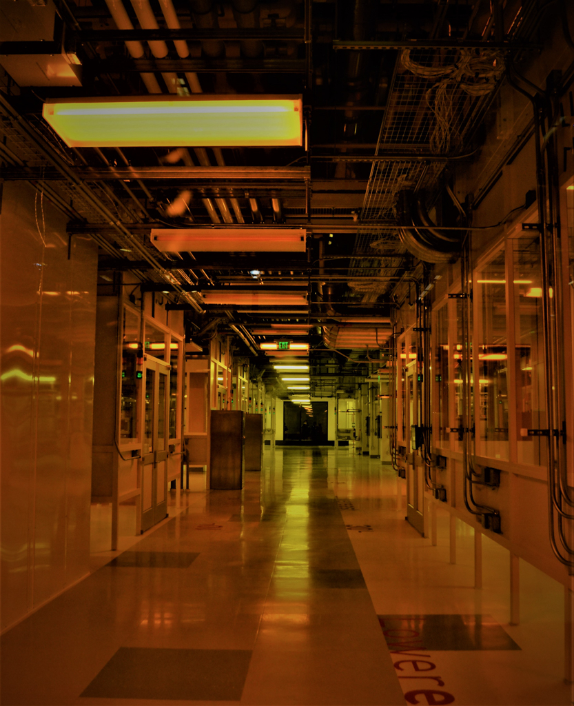
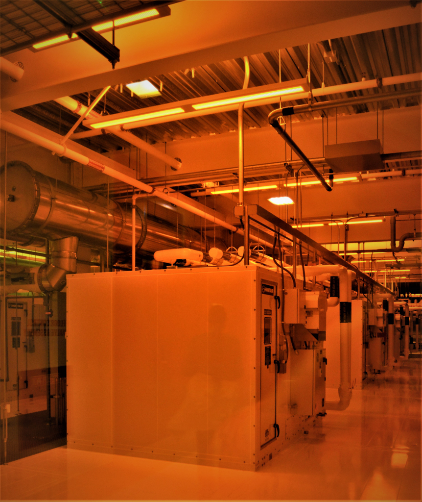
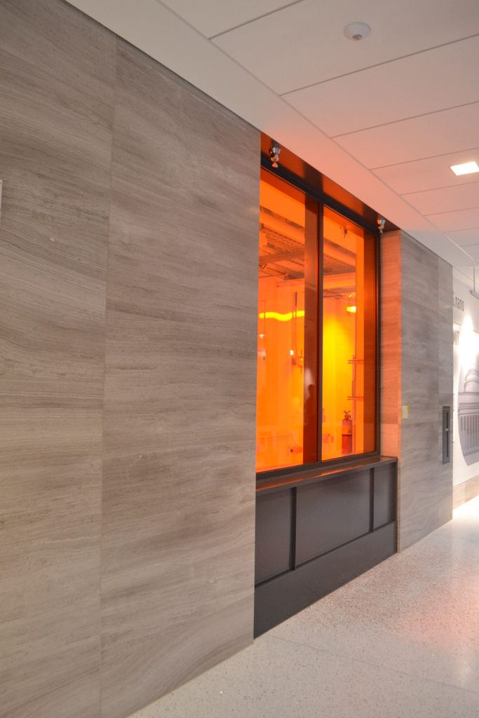
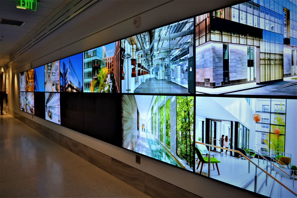
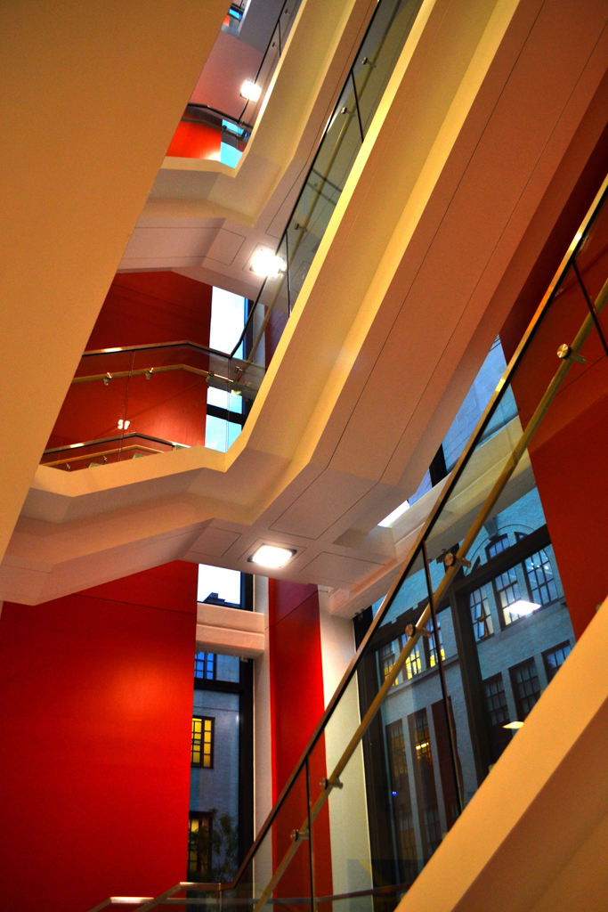
MIT’s hub for nanoscale research is a cutting-edge facility that incorporates hundreds of overlapping building systems to precisely maintain air cleanliness, temperature, humidity, noise, and vibration—all in curtainwall exterior that puts the research occurring within on display. Wilson Architects (now Wilson HGA) likens the project to building “a Ferrari engine under a glass hood.” Nanoscience is the study of matter at nanoscale dimensions, that is, one-billionth of a meter (for context, a single human hair is approximately 80,000–100,000 nanometers wide). This work requires a specific environment, one that is usually isolated from outside interference. MIT.Nano, however, is part of an urban campus, located along the “Infinite Corridor,” the campus’s central spine. Yet the precision with which the building is executed makes nanoscale research possible even in such a bustling environment.
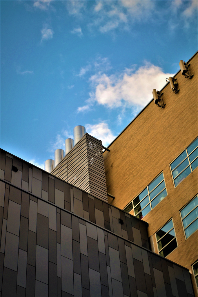
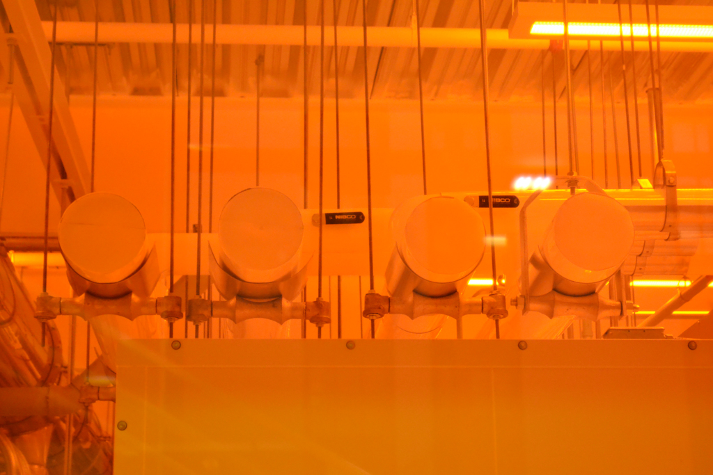
For its sustainable design, the architects selected highly durable and long-lasting materials such as stone cladding, fiber cement boards, terrazzo flooring, certified lumber and lower embodied carbon insulation. The building program includes high-performance cleanrooms, 100,000 square feet of lab spaces, new undergraduate chemistry teaching labs, an immersion lab, a two-story virtual reality space, meeting spaces, and an outdoor courtyard. One of the leading requirements for MIT.Nano’s design and operation is an integrated system with flexible connection for mechanical and electrical services, isolated foundations, and active electronic isolation systems to maintain the precise environment needed to conduct research at nanoscale. For example, the cleanrooms’ exterior envelopes are air-tight and the curtainwall system has reinforced thermal breaks to prevent condensation. Within its energy-efficient cleanrooms, the air is continuously replaced to maintain its required standard.
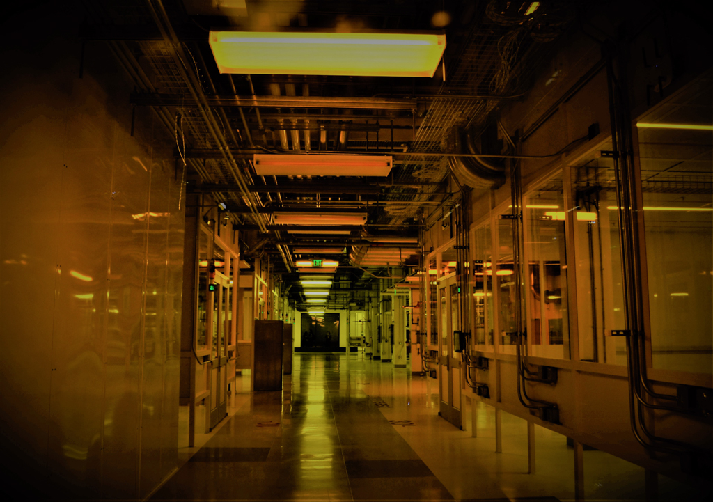
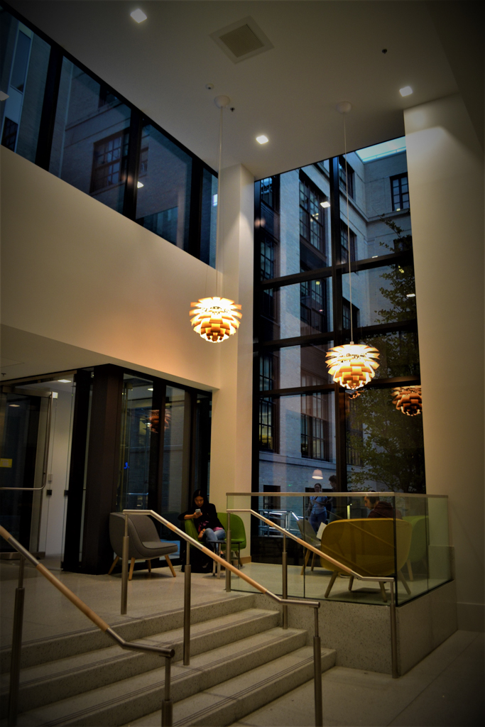
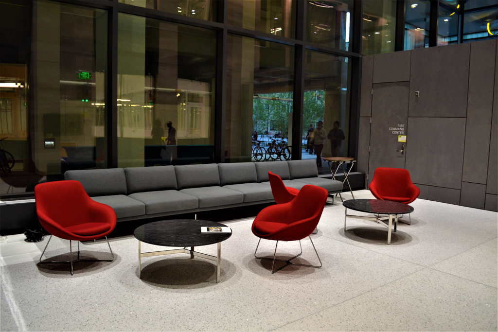
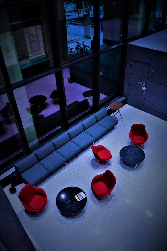
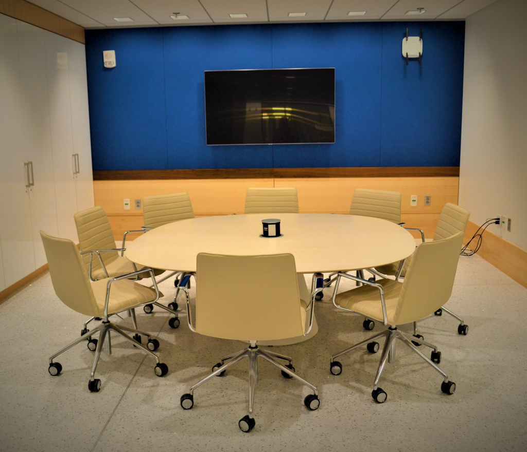
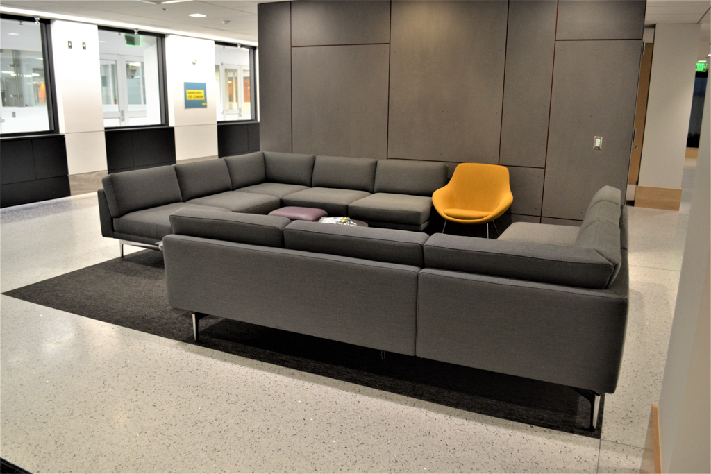
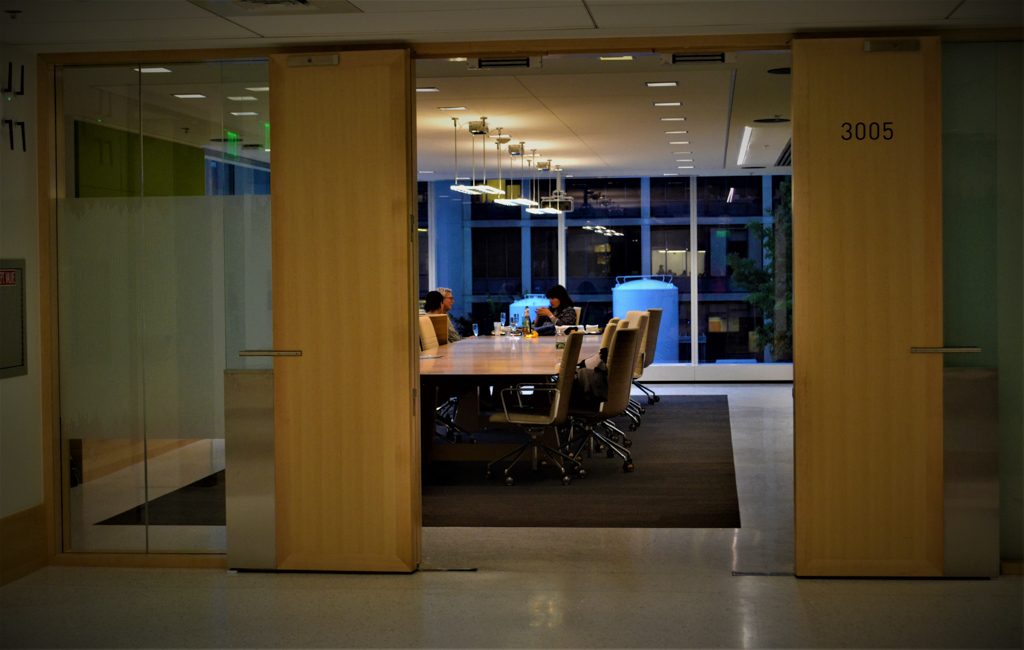
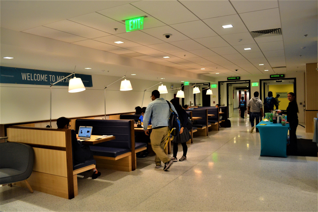
A major goal of MIT.Nano’s design team is to foster collaborative and multidisciplinary research while also considering the unknown future of scientific research in relevant fields. MIT.Nano’s modular design, therefore, allows for variation and flexibility of spatial arrangements and organizations over time, including expansion. Instead of belonging to a department, its interior includes shared research environments, world-class laboratories, two levels of class 100 and 1,000 cleanrooms, and meeting spaces. Cleanrooms were designed to allow visual connections between these spaces, their occupants, and all visitors. In addition, well-lit interior corridors with daylight are supportive design components for interaction of its community, like primary circulation paths that include strategic gathering spaces.
The design team focused efforts on energy-use reduction, and incorporated over 60 energy conservation measures that ultimately led to a LEED Platinum certification. These measures include: controlled lighting and temperature systems, including occupant-operated thermostats, desk fans, and sunshades; infrastructure systems for water and stormwater treatment; resiliency for potential flooding by relocating electrical switchgear and an emergency generator on the uppermost level; and emergency backup systems in the event of extreme weather. MIT.Nano saves more than 50 percent in energy costs by reducing its carbon footprint, making it one of the most energy-efficient buildings in the field.
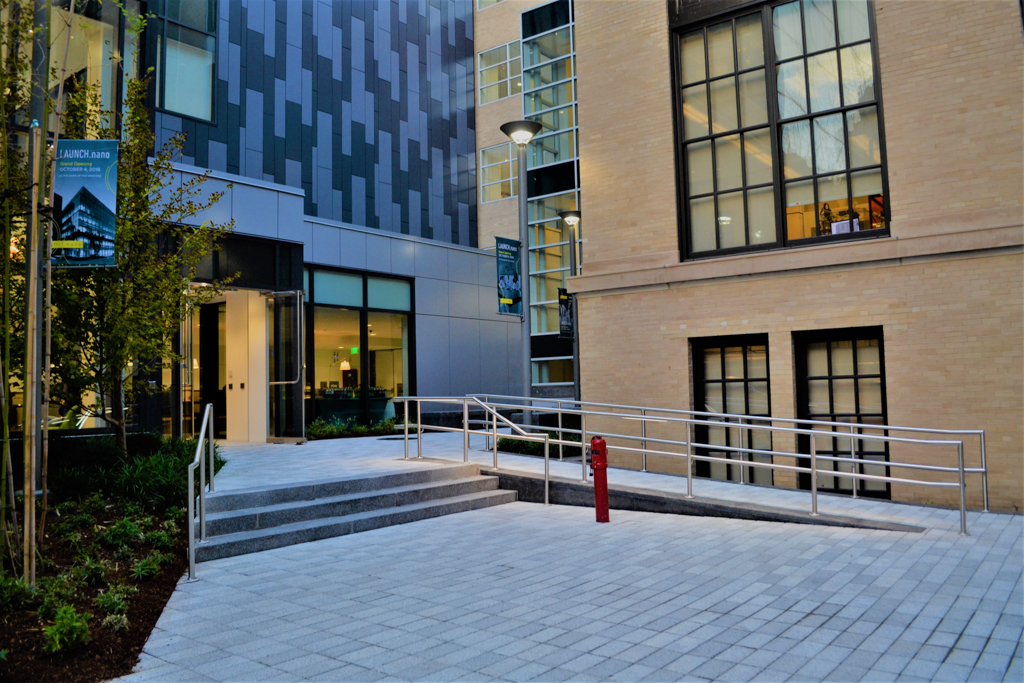
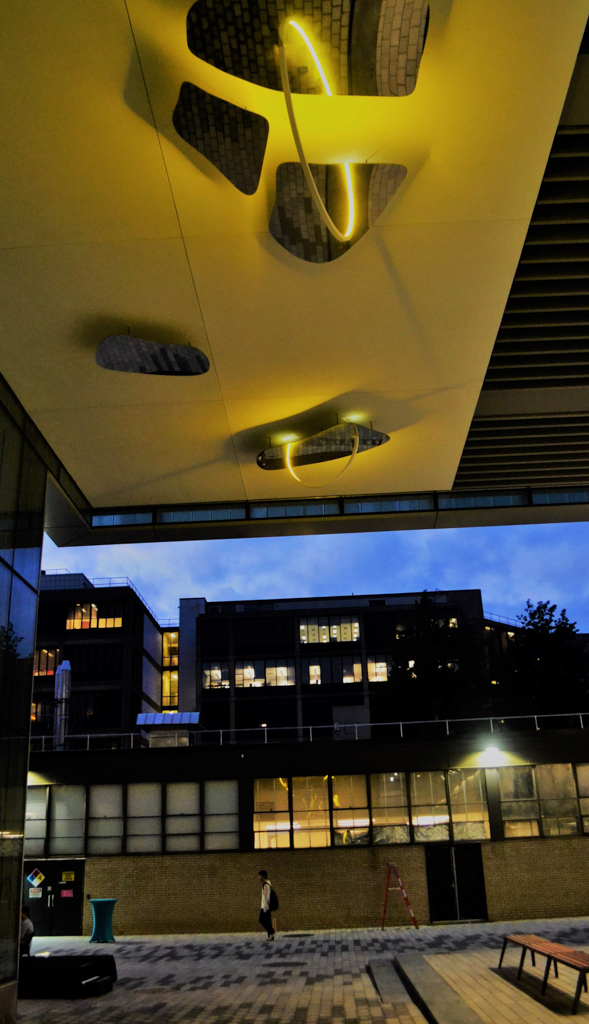
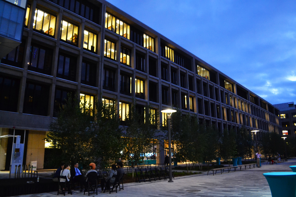
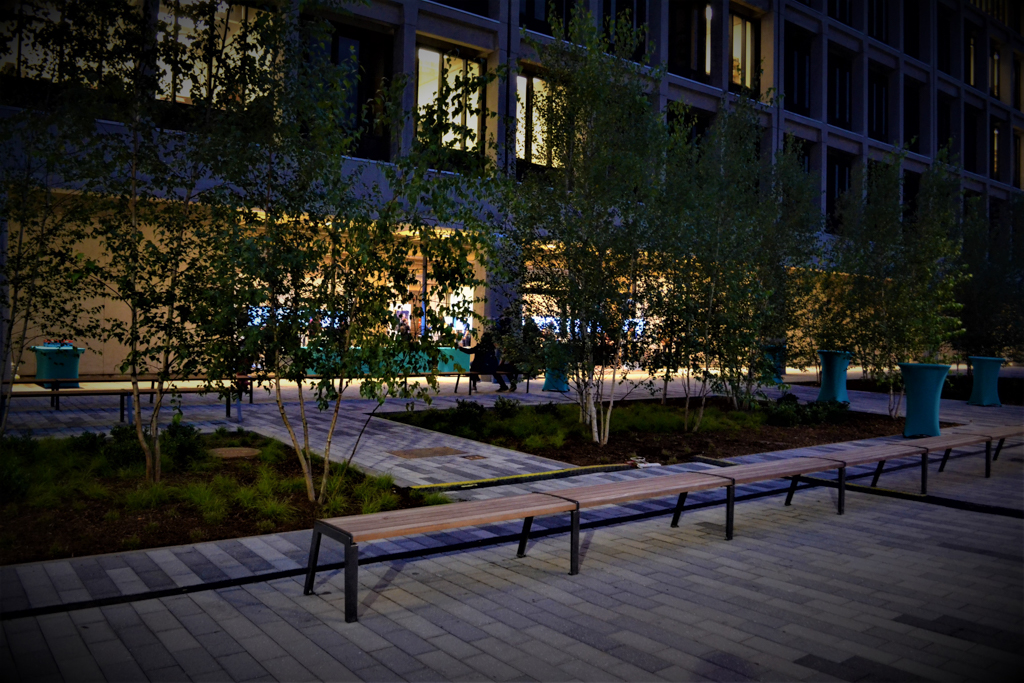
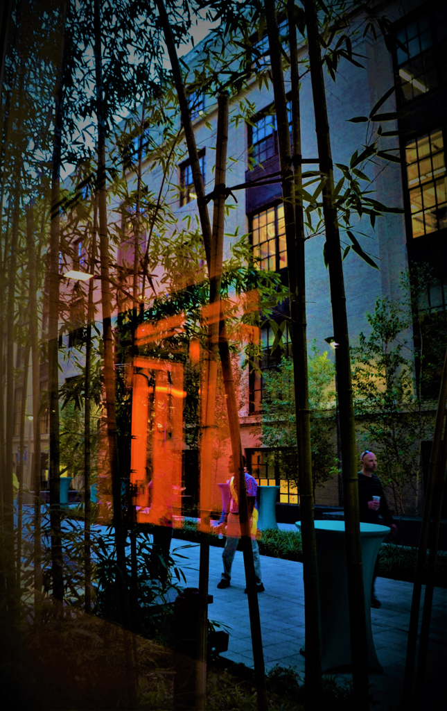
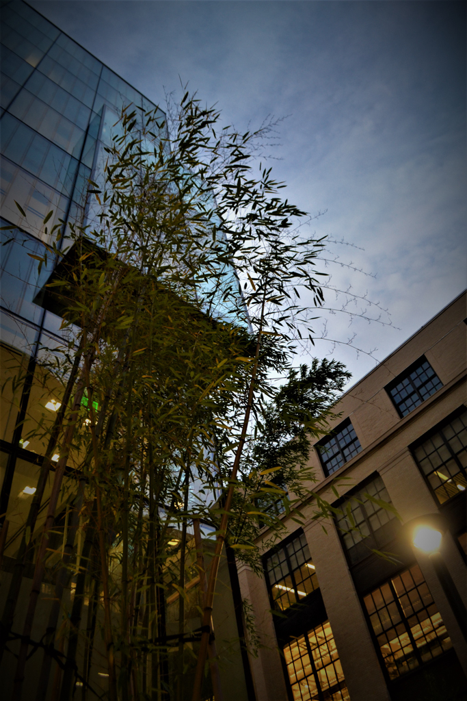
The outdoor spaces contain a network of walkable areas. Of note is the Improbability Walk, a courtyard path located on the south side of the building that honors late MIT Professor Emerita Mildred Dresselhaus, a pioneer in solid-state physics and nanoscale engineering. This pedestrian-friendly outdoor space includes several seating areas, seasonal plantings, garden lighting, and over 100 trees. On the breezeway ceiling between the Improbability Walk and the North Corridor is North West Passage, a site-specific art installation by Olafur Eliasson. The rounded forms of Eliasson’s work, created using stainless steel and LED lights, refer to the silhouettes of free-floating ice between North America and the Arctic Circle—a commentary on climate change.
MIT.Nano’s exemplary construction resulted in many awards and accolades, such as an American Institute of Architects Annual COTE award (2021), Boston Society of Architects Honor Award for Design Excellence (2020), the International Institute for Sustainable Laboratories (I2SL) “Go Beyond” Award (2019), the American Institute of Architects Education Facility Design Award of Merit (2019), the American Council of Engineering Companies of Massachusetts (ACEC/MA) (2019), and the Research & Development World Lab of the Year Award (2019).